Surface Texturing
Surface texturing, either in combination with an anti-reflection coating or by itself, can also be used to minimize reflection. Any "roughening" of the surface reduces reflection by increasing the chances of reflected light bouncing back onto the surface, rather than out to the surrounding air.[Dale1960]
 Surface texturing can be accomplished in a number of ways. A single crystalline substrate can be textured by etching along the faces of the crystal planes. The crystalline structure of silicon results in a surface made up of pyramids if the surface is appropriately aligned with respect to the internal atoms. One such pyramid is illustrated in the drawing below. An electron microscope photograph of a textured silicon surface is shown in the photograph below. This type of texturing is called "random pyramid" texture[Bailey1979], and is commonly used in industry for single crystalline wafers.
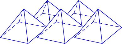
A square based pyramid which forms the surface of an appropriately textured crystalline silicon solar cell.
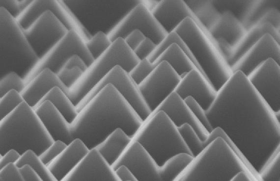
Scanning electron microscope photograph of a textured silicon surface. Image Courtesy of The School of Photovoltaic & Renewable Energy Engineering, University of New South Wales.
Another type of surface texturing used is known as "inverted pyramid" texturing[Campbell1987],[Campbell2001]. Using this texturing scheme, the pyramids are etched down into the silicon surface rather than etched pointing upwards from the surface. A photograph of such a textured surface is shown below.
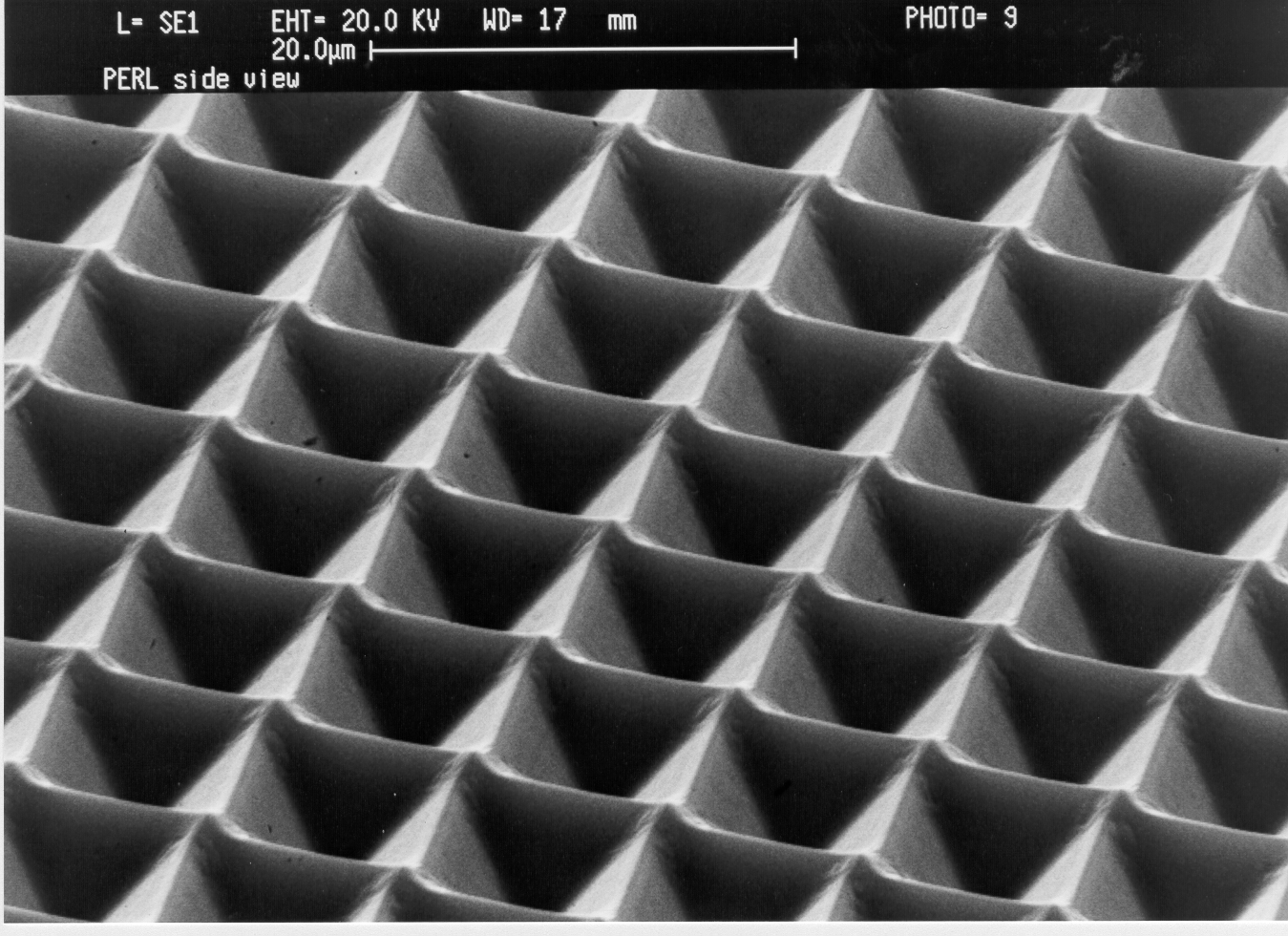
Scanning electron microscope photograph of a textured silicon surface. Image Courtesy of The School of Photovoltaic & Renewable Energy Engineering, University of New South Wales.
For multicrystalline wafers, only a small fraction of the surface will have the required orientation of <100> and consequently these techniques are less effective on multicrystalline wafers. However, multicrystalline wafers can be textured using a photolithographic technique[Zhao1991] as well as mechanically sculpting the front surface using dicing saws[Wenham1988] or lasers[Zolper1989] to cut the surface into an appropriate shape. A micrograph of a photolithographic texturing scheme is shown below.
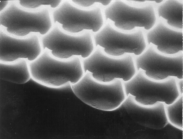
Scanning electron microscope photograph of a textured multicrystalline silicon surface. Image Courtesy of The School of Photovoltaic & Renewable Energy Engineering, University of New South Wales.
The modeling of textured substrates is covered by simulation programs at pvlighthouse.com.au and associated references[533]
References
Section titled “References”- B. Dale and H.G. Rudenberg, “High efficiency silicon solar cells,” U.S. Army Signal Research and Development Lab, pp. 22, 1960.
- W. Bailey et al., “United States Patent: 4137123 - Texture etching of silicon: method,” 1979. http://patft.uspto.gov/netacgi/nph-Parser?Sect1=PTO2&Sect2=HITOFF&p=1&u=%2Fnetahtml%2FPTO%2Fsearch-bool.html&r=32&f=G&l=50&co1=AND&d=PTXT&s1=4,137,123&OS=4,137,123&RS=4,137,123
- P. Campbell and M. Green, “Light trapping properties of pyramidally textured surfaces,” Journal of Applied Physics, vol. 62, no. 1, pp. 243, 1987. https://doi.org/10.1063/1.339189
- P. Campbell and M. Green, “High performance light trapping textures for monocrystalline silicon solar cells,” Solar Energy Materials and Solar Cells, vol. 65, no. 1-4, pp. 369 - 375, 2001. https://doi.org/10.1016/S0927-0248(00)00115-X
- J. Zhao et al., “Improvements in silicon solar cell performance,” pp. 399-402, 1991.
- S. Wenham and M. Green, “Buried contact solar cell,” 1988. http://www.freepatentsonline.com/4726850.html
- J. Zolper et al., “16.7% efficient, laser textured, buried contact polycrystalline silicon solar cell,” Applied Physics Letters, vol. 55, pp. 2363, 1989. https://doi.org/10.1063/1.102019
- S. Baker-Finch, K. McIntosh and M. Terry, “Isotextured Silicon Solar Cell Analysis and Modeling 1: Optics,” IEEE Journal of Photovoltaics, vol. 2, no. 4, pp. 457 - 464, 2012. https://doi.org/10.1109/JPHOTOV.2012.2206569