Example 1: General Solution for Wide Base P-N Junction
Overview
- Situation where the solar cell surface is far enough away from the junction edges that recombination properties of carriers injected into the quasi-neutral region under forward bias are not impacted.
- The boundary conditions for the wide base diode particular solution are:
(1) At the edge of the depletion region,
(2) minority concentration is finite (B=0) - Total Current is therefore:
A wide base junction is one in which the surface are far away enough from the junction edges such that they to not impact the recombination properties of carriers injected into the QNR under forward bias.
Step 1: Solve for properties in depletion region
Section titled “Step 1: Solve for properties in depletion region”As in most devices, the solution for the electrostatic properties in the depletion region does not change, and so is not repeated.
Step 2: Solve for carrier concentrations and currents in quasi-neutral regions
Section titled “Step 2: Solve for carrier concentrations and currents in quasi-neutral regions”
The solution below is shown in detail only for the n-type material (in which there is a hole current).
Find U and G
Section titled “Find U and G”We will set G equal to a constant and in the n-type material (in p-type material, ).
Find general solution
Section titled “Find general solution”Using low injection recombination and constant generation gives the equation:
Note that ,
since
(where pn0 is a constant), so the derivative (and second derivative) of Δp(x) is the same as the derivative of p(x). In addition for simplicity, we introduce a variable change using: .
The overall differential equation now becomes:
or
which has the general solution:
For electrons (p-type material), the differential equations and solutions are:
and
Particular solution for wide base diode
Section titled “Particular solution for wide base diode”We need two boundary conditions these are:
(1) At the edge of the depletion region,
(2) The minority carrier concentration must be finite even as x tends to infinity. This can only be achieved if B = 0.
Since B = 0, the general solution for holes then becomes
at x = 0
Rearranging gives:
Plugging A back in gives:
or
The equation for electrons in p-type material, Δn(x') , can be similarly derived as:
This is plotted below for G=0.
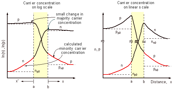
Differentiating and plugging into equation for current gives:
Making the change from x to x' gives
Step 3: Finding total current
Section titled “Step 3: Finding total current”The change in the current across the depletion region is:
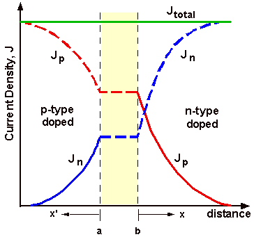
Assuming that there is no generation and recombination, then ΔJn = 0 and
This case is shown in the graph below.
If there is a constant generation across the depletion region, then , where xn is the depletion width in the p-type material and xn +xp = W.
Jn at the edge of the depletion region in the p-type material is:
Jn at the edge of the depletion region in the n-type material is:
An analogous equations exists for Jp, and the total current is:
Typically, we write the equation in the form:
or
where